Additive manufacturing technology has become a pioneer for many developments to come in the future. With improvements in 3D applications and printing technology, experts have been able to make 3D printing a viable choice for manufacturers.
It is no more just a good invention rather a technology that is impacting different industries around the globe. Amid these innovations, Nanoscale 3D printing is a lesser-known development that possesses huge potential to further the quality of printed parts while offering high throughput.
With time, 3D printers are becoming affordable. Moreover, individuals are showing great interest in learning about the technology. Hence, to make the printing experience to an altogether next level, the experts from Lawrence Livermore National Laboratory (LLNL) and the Chinese University of Hong Kong have come up with a unique idea for printing nanostructures.
Using a unique time-based technique that helps tame light from an ultrafast laser, the researchers are able to achieve dramatically faster printing rates with Nanoscale technology.
According to the various reports, this novel approach can easily help speed up the fabrication process. Not just by a small difference, but achieving a thousand times faster speed than the current method, i.e., TPL (two-photon lithography) processes. In addition, Nanoscale 3D printing will not compromise the resolution of the parts for printing at such a rapid rate.
What is Nanoscale 3D Printing?
Did you notice that the size of electronics is becoming sleeker over the years? Thanks to microfabrication which aims at fabricating miniature models of micrometer scales and even tinier.
Think of decreasing the size of the components from tens of micrometers down to just tens of nanometers. Hence, soon, microfabrication was given a new name, nanofabrication. However, these two approaches share the same governing principles. The trend offered industries an opportunity to manufacture products that occupy less space and are lightweight.
However, the process isn’t that simple. Moreover, for meeting the challenges of shrinking the size of components, experts needed innovative techniques, capable of scaling continually. And, among the various alternatives, Nanoscale 3D printing seemed the best choice for the faster production of tiny structures.
Very similar to the SLA 3D Printing technique, Nanoscale 3D printing also employs light sources to harden the photosensitive resins. However, the process brings many improvements to the existing SLA technology to offer better resolution and faster speed.
Technology Behind Nanoscale 3D Printing
The manufacturing of nanostructures gained momentum after the introduction of the two-photon lithography process. Abbreviated as TPL, the technique helped industries immensely in the creation of nanoscale 3D structures.
However, there were limitations in the TPL process that restricted the resolution and speed of chemistry. In other words, one is required to trade-off between resolution and speed.
Therefore, to continue development within Nanoscale 3D printing, the experts came up with a new approach, called FP-TPL (femtosecond projection TPL).
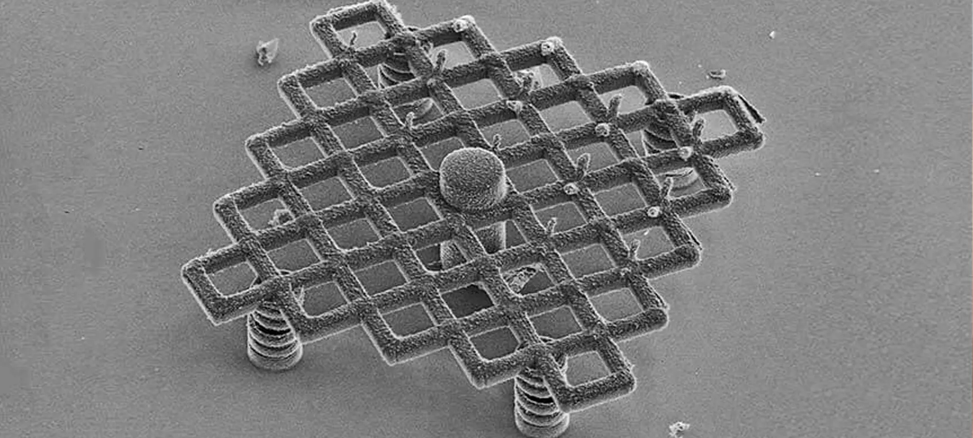
The development led to various improvements to the existing TPL approach. Not just the faster printing speed, but FP-TPL can print nanostructure with a depth resolution of 175 nanometers. Further, it can help produce geometries carrying 90 degrees overhangs, otherwise impossible or complex to create.
TPL vs FP-TPL
Yes, we can create higher resolution nanostructures without compromising the speed of production. Thanks to the FP-TPL process that is an improved version of the conventional TPL technology. So, how exactly do these two approaches differ?
Among the various differences, the major one lies in the way the light source is exposed to the build surface. In FP-TPL, to achieve greater throughput, the machine employs million of light points focused simultaneously.
On the contrary, the TPL approach depends on a single high-intensity spot of light ranging between 700 to 800 nanometers in diameter. This light source, when exposed to the photosensitive polymers, hardens the material layers, one by one.
Although the TPL process has been in practice for long, its effectiveness is blurred with longer print times. And, the production time keeps surging with the structure’s complexity.
To be candid, TPL can take hours to 3D print complex 3D structures. Hence, it stays highly limited when it comes to scalability. This is due to the fact that the process relies on the point for scanning through the entire printed structure.
When talking about FP-TPL, the machine projects millions of points at once. Hence, scaling up the printing process exponentially. Instead of using a single high-density point of light, FP-TPL utilizes a complete plane of projected light. Therefore, rather than aiming at a single point, users can focus on the entire plane, creating the patterns simultaneously into arbitrary structures.
How is FP-TPL Accomplished?
The development is really monumental. With the FP-TPL approach, users now can achieve high resolution at a faster speed too. However, how does that happen?
As mentioned, the technique uses a million light points at once. Hence, to create the plane of lights, experts innovated a digital mask, something very similar to the ones found in projectors. In addition, the plane of projected lights does not trace images.
On the contrary, the digital mask takes over the control of the femtosecond laser for creating desired light patterns over the liquid resin. Finally, solidifying the layer of the parts.
According to the researchers, the digital mask helps in offering high-resolution parts. With each layer printed using a 35-femtosecond burst of high-intensity light, the resultant nanostructure turns out to be very accurate and precise.
As it’s the case with the additive manufacturing technique, the layer solidification is repeated, forming one layer at a time. And, it continues until the users get their complete 3D structure constructed.
Talking about speed, the 3D structures can print in around 8 minutes. Isn’t that a drastic difference when compared to the TPL process which usually takes hours for creating nano parts?
Benefits of FP-TPL, Nanoscale 3D Printing Approach
We have already been discussing a lot of benefits that the new approach brings with itself. However, there is more to the story. The technique will not only help users increase their production throughput, but will bring more versatility for their projects in terms of material, resolution, and more.
Better Geometries
FP-TPL, the latest nanoscale 3D printing technology is capable of projecting the laser at any height into the photopolymer, regardless of the depth of the material. Hence, enabling the production of new designs with geometries that weren’t possible before. For instance, the designs with 90-degree overhangs, or those with aspect ratios of length to feature size of 1,000:1.
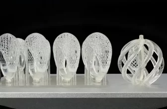
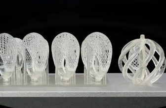
All this is possible with the help of FP-TPL technology. Not just the better quality but the creation of impossible designs is really a huge leap for the nanoscale 3D Printing niche. The process makes it easy to print difficult designs such as cuboids, micro-pillars, log-piles, spirals, and wires.
Greater Material Choice
Those behind the development of FP-TPL technique believe that this approach won’t be limited to just photopolymers. However, in the coming future, the technology will adapt to the requirements of metals and ceramics for adding more materials for versatile results when manufacturing using nanoscale 3D printing.
By generating the materials from precursor polymers for metal and ceramic printing, the technology will become accessible for an even larger number of industrial applications.
In short, the process will allow the printing of nano components using a larger material palette that could be incorporated with larger devices.
No More Trade-Offs
3D Printing is a revolutionary innovation. However, it comes with its own baggage of limitations. And, the major one being the unavoidable trade-off that users have to make between speed and resolution.
For achieving higher resolution, one must compromise with speed. However, those looking to create parts at a faster pace must overlook the discrepancies in the part quality.
However, with nanoscale 3D printing, these trade-offs do not stand a chance. The latest FP-TPL approach enables printing at a thousand times faster speed compared to the traditional methods. In addition, allowing printing with the smallest of features.
Application of Nanoscale 3D Printing
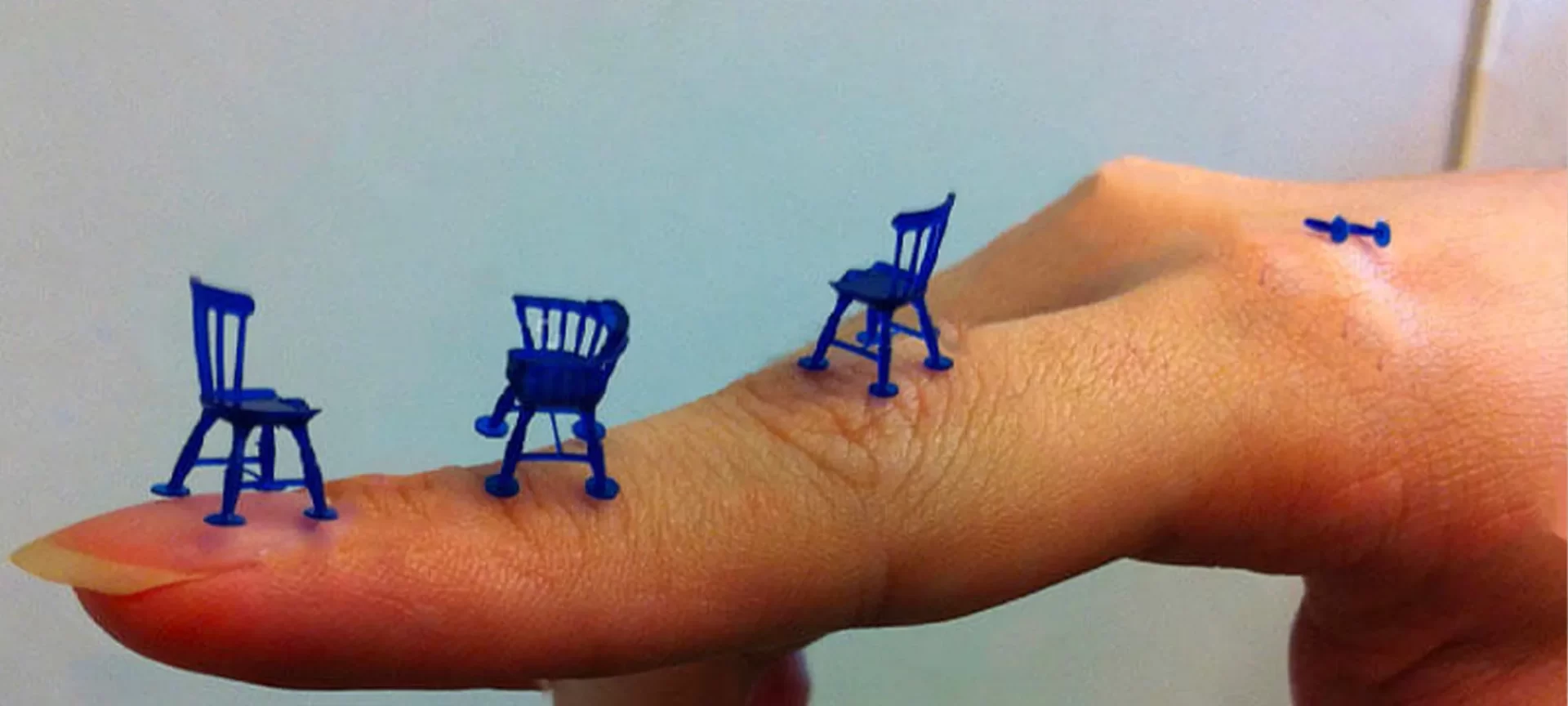
When it comes to applications of Nanoscale 3D printing, the process can help many industries reshape their production regimen. Allowing users to shrink their product’s components to nano sizes, the process can help create parts that are smaller and lighter. So, here are some of the examples of industries that are already making use of the technology.
Electronics
As you may expect, nano 3D printing can drastically improve functionality as well as performance within the electronic sector. Enabling the miniaturization of devices, companies can come up with better and efficient products for their customers.
In addition, engineers can benefit through faster lead times when testing prototypes. When it comes to innovation, testing new components often takes a lot of time, especially when you need to outsource the production of prototypes.
However, with in-house prototyping rather than depending on outsourcing, manufacturers can complete the tests for new designs in less time. Moreover, the technology offers flexibility and customization for simplified supply chains.
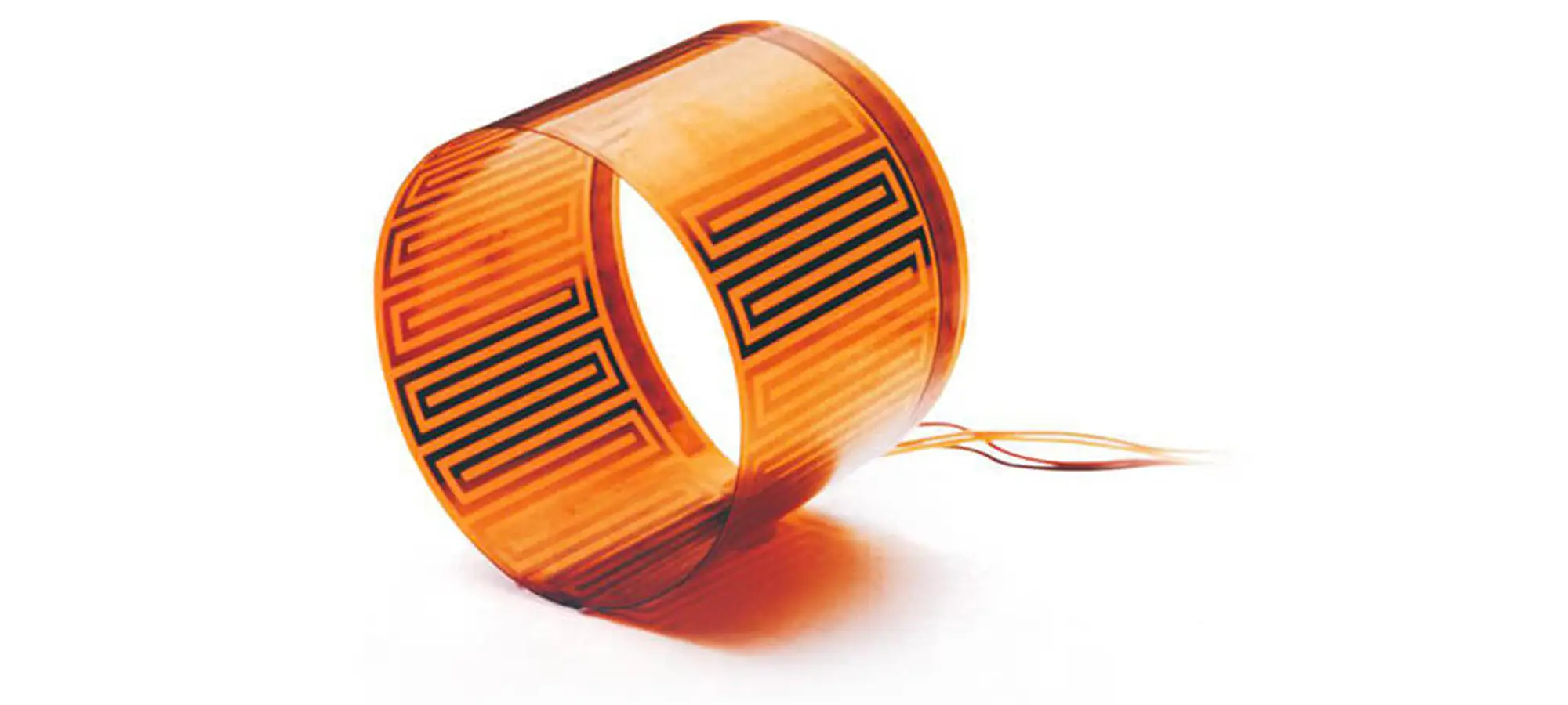
Using the technology, electronic sectors can create multi-layer PCBs (Printed Circuit Boards), embedded electronics, antennas, electromagnets, MIDS (Molded Interconnect Devices), sensors, and more.
Aerospace and Automobile
With current demands, it is obvious that researchers from different fields are looking forward to what additive manufacturing can accomplish. And, when it comes to nanoscale 3D printing, the demands only keep surging.
Industries such as aerospace and automobiles prefer parts and components with low volumes. For instance, lighter components in airships make the design more efficient and safer.
The same goes for the automobile sector. The companies manufacturing cars and vehicles need nano components to boast the design of their overall products.
Other Sectors
Well, it is lucid that almost every sector needs components that are tinier in size. From medical to defense, nanoscale 3D printing can benefit a huge number of sectors with its amazing manufacturing techniques.
Multiple startups and new companies are already trying their luck with nanoscale 3D printing. For instance, companies like Microfabrica, Boston Micro Fabrication, Nanoscribe, or MicroLight3D have come up with their version of nanoscale 3D printing techniques for creating medical devices.
While operating on patients, medical professionals aim to minimize the amount of collateral tissue damage to as little as possible. And, this is possible with miniaturizing medical devices.
In short, the technology can find its application for producing micro-optics, electrochemical interfaces, flexible electronics, mechanical metal materials, optical metamaterials, bioscaffolds, and other functional nanostructures.
Future for Nanoscale 3D Printing
While we are still in the nascent stage, nanoscale 3D printing has already made its way within various industries. Its application is not going to be limited to a few sectors. However, in the future, the probable applications may include embedded sensors or wearables for monitoring health in real-time.
Moreover, 3D printed sensors for lenses produced with nanoscale printing may enable users to experience augmented reality applications. In addition, 3D printed embedded electronics may find their place within varied products. From cars to mobile phones to laptops, nano components have the potential to add functionality while keeping the design lighter.
The Conclusion
We have seen the various hurdles and limitations that other 3D printing processes have to go through before becoming accessible. And, for wider adoption, Nano printing will have to meet similar challenges.
However, the fact will remain unchanged. 3D printing applications across different niches and for variable part size production will only continue to become more valuable with time. From engineering parts to designing prototypes, nano printing will be a treasured addition to additive manufacturing technologies.
It is imperative to understand the benefits this technology brings, offering some new and unique tools for engineers who struggled with complex designs previously. In addition, the technology aims at reducing the cost for production of nanostructure which is very expensive otherwise.
To conclude, the wider adoption of nanoscale 3D printing isn’t impossible. Once the technology fights with the limitations concerning today, it will surely find its place among different industries on a larger scale.
Once we have intuitive applications for designing 3D models for such small manufacturing along with an expanded material palette, the progress will start soaring right away.